TDK-Lambda KPSA Power Supply
The Lambda KPSA10-15 is a self-contained, offline power supply capable of supply 15Volts DC at 1 Ampere from a universal input of 120VAC ~ 240VAC, 50/60Hz. It is designed for PCB mounting as a module and is passively cooled. Several of these power supplies failed in the field in 2-2.5 years. There was no sign of damage or environmental contamination on the PCB. All arrived DOA. The component selection was mediocre except for the electrolytic capacitors, which were chosen wisely.
After carefully applying a bias to the failed unit it was confirmed that the unit would not power-on. No switching activity of any type was observed across the transformer primary, and no voltage was produced at the secondary windings. The components in the power stage were tested and functioning. Subsequent ‘AB’ testing between the defective unit revealed a low-impedance path from VDD to GND on IC1, reading roughly 50 ohms. On the functional unit, this figure measured open-circuit. Additionally, the GATE output of IC1 also exhibited a low-impedance path to GND, whereas the functional unit measured near open-circuit in this position.
After removing IC1 from the defective unit, switching MOSFET Q1 was confirmed to be undamaged, showing no signs of leakage across any pins. This pointed to one of two potential causes, the first being a failure of IC1 due to a quality issue, the second being electrical overstress on the VDD line. A DMM was used to verify that D1 and R1 and C1 were intact, as these three components, along with a dedicated winding from T1, form the basis of the VDD bias circuit. An LCR bridge was used to compare C1 on both the functional and non-functional units. In both cases, the capacitor measured 8.0uF with a 3.0 ohm ESR, both reasonable figures for this type of component.
No component defects other than IC1 were found.
IC1 appears to be of unknown origin, marked with a reference number of ‘RS2042’. It appears that this power controller is made by one of two companies, either ‘Orister Semiconductor’ or ‘Princeton Semiconductor’.
In order to rule out electrical overstress on the VDD line as a likely cause, the functional unit was powered up and two related nets were observed with an oscilloscope during operation. These two nets included the VDD to GND signal as well as the GATE to GND signal. Measurements were made at a series of operating points, including No Load, Full Load, Turn On, Turn Off, 50% Load Step Up, 50% Load Step Down, and Output Short Circuit. A 100MHz isolated high-voltage differential probe was used for all measurements. All measurements were made with an input voltage of 208VAC.
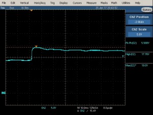
The VDD to GND signal was found to range from between 16VDC to 20VDC, generally reading higher with higher connected load, as this would cause a larger pulse width on the primary switch. The datasheet upper non-damaging limit for VDD is 40VDC. The datasheet also indicates that the IC will lock-out from over-voltage if VDD exceeds 24VDC. Additionally, AC ripple was measured across this net, showing roughly 100mVp-p of ripple, which is normal for the application. There were no concerns.A large load step upwards seemed to produce the highest recorded value on VDD, as shown in the plot below:
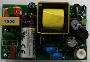
KPSA -15 Power supply
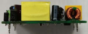
back view
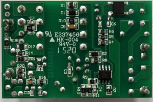
Top side view
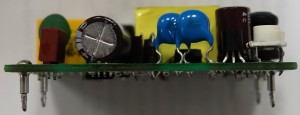
Power supply side
Waveform