Potential Contamination Photodiode
Gideon Analytical Laboratories received several photodiodes to examine for possible contamination. A diode is a two-terminal electronic component with asymmetric conductance. It has low resistance to current flow in one direction, and high resistance in the other direction. There are various kinds of diodes, including vacuum tube diodes and solid state diodes. The most used and ubiquitous diode is the semiconductor. A photodiode is a type of device capable of converting light into either current or voltage. Gideon Analytical Laboratories was requested specifically to examine the gold bond pads for possible contamination.
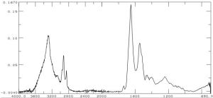
Failure analysis ensued. First, seven of the photodiode gold pads were cross-sectioned to prepare for examination under a stereo-zoom microscope, and later for SEM-EDS and FTIR analysis. Examination under the stereo-zoom microscope yielded no detectable layer of contaminant on the surfaces of the gold bonding pads. There were only some small particles on them. Many micrographs were taken on each pad using SEM; there were a few noticeable spots on the pads. These spots were analyzed using EDS. There was gold. Also present was tungsten, copper, and some silicon were found in very small amounts. SEM-EDS analysis was also conducted on the solder bump. Copper was present, but not enough to cause any problems. Overall analysis of the photodiode gold pads included over 50 SEM-EDS scans and all showed nearly identical spectra. There were normal levels of all elements were supposed to be there. The presence of other elements was negligible at best; these photodiodes were free of contamination.
Gideon Analytical Laboratories can preemptively test devices before they fail in the field. We can perform quality assurance for your devices that will save your company time and money. Quality assurance is extremely important; if you have questions regarding contamination, moisture, or passivation, call us for testing so that you know your devices are working properly. If there are any problems in design, production, or application, Gideon Analytical Laboratories is here to help.
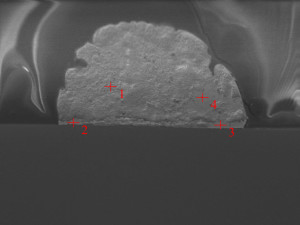
micrograph of solder bump

SEM-EDS of solder bump, lead and indium
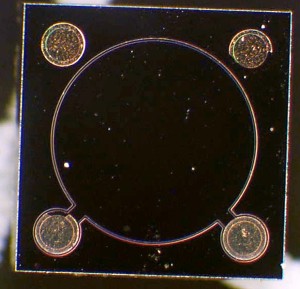
Photodiode, gold pads
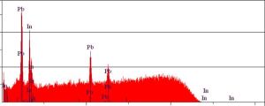
SEM-EDS of solder bump, lead and indium
gold pad
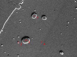
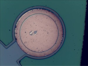
micrograph; particles on a gold pad
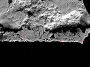
micrograph of right corner of solder bump
FTIR scraping from a gold pad